The semiconductor industry designs chips the same way it did a decade ago. That's about to change.
Every chip you use went through a process that would horrify anyone in software engineering. A team of 10 to 50 engineers spent 12 to 18 months manually iterating on a design. Place blocks, run simulations, stare at timing reports, move things around, run it all again. Hundreds of iterations. Millions of dollars. All before a single chip was fabricated.
Most of that iteration is wasted.
Software ships in hours. Chips ship in months. The difference isn't complexity, it's automation.
The Physical Design Bottleneck
Chip design has two halves. The frontend, writing RTL and verifying logic, has seen massive improvements. Agentic coding tools like Cursor and Copilot are accelerating it even further.
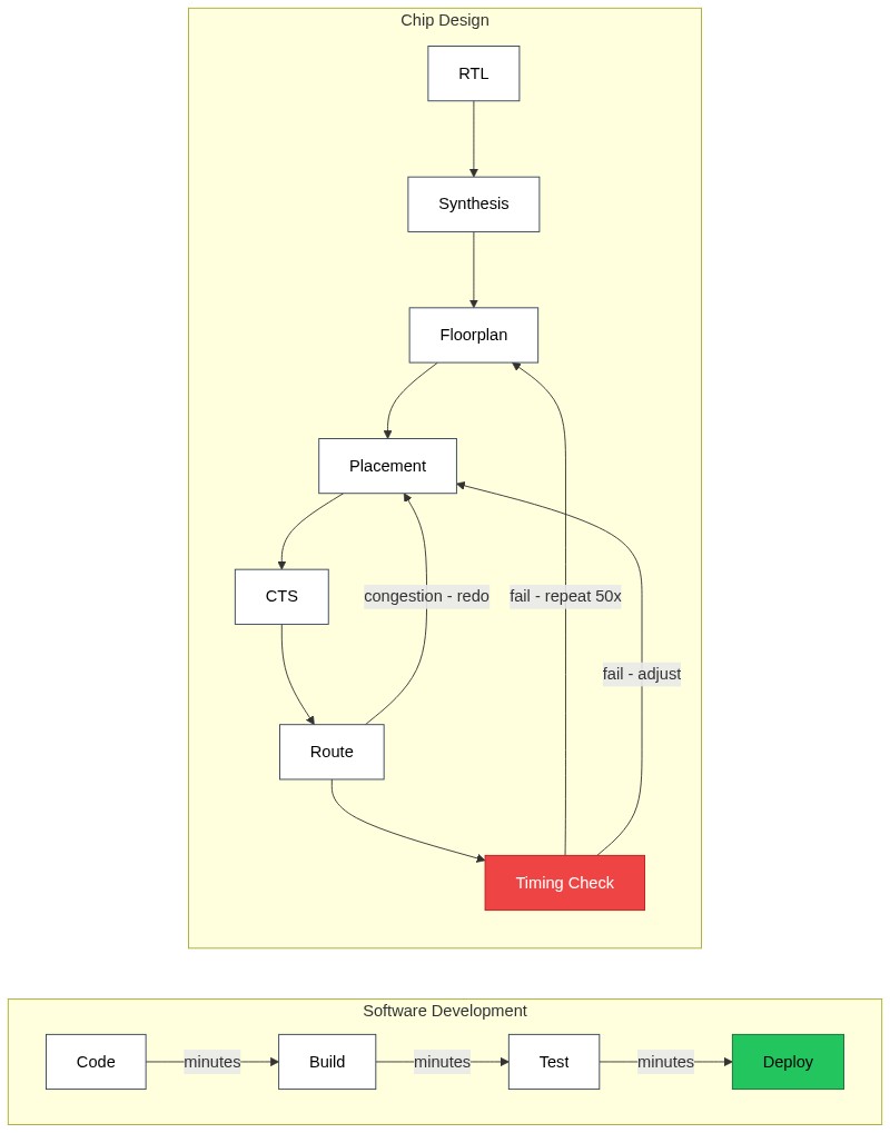
The backend, physical design, is where verified logic becomes an actual layout of transistors, wires, and metal layers that meets timing, power, and area targets. It consumes nearly 60% of the design cycle, with minimal AI support. This is where projects stall.
An engineer places macro blocks on a floorplan, runs a flow that synthesizes, places standard cells, builds a clock tree, routes wires, and checks timing. That takes 30 minutes to 8 hours. Then: "Timing violation on path group CLK, worst slack -0.4ns." Move a macro. Re-run. Wait. Check. Move again. This loop repeats for weeks.
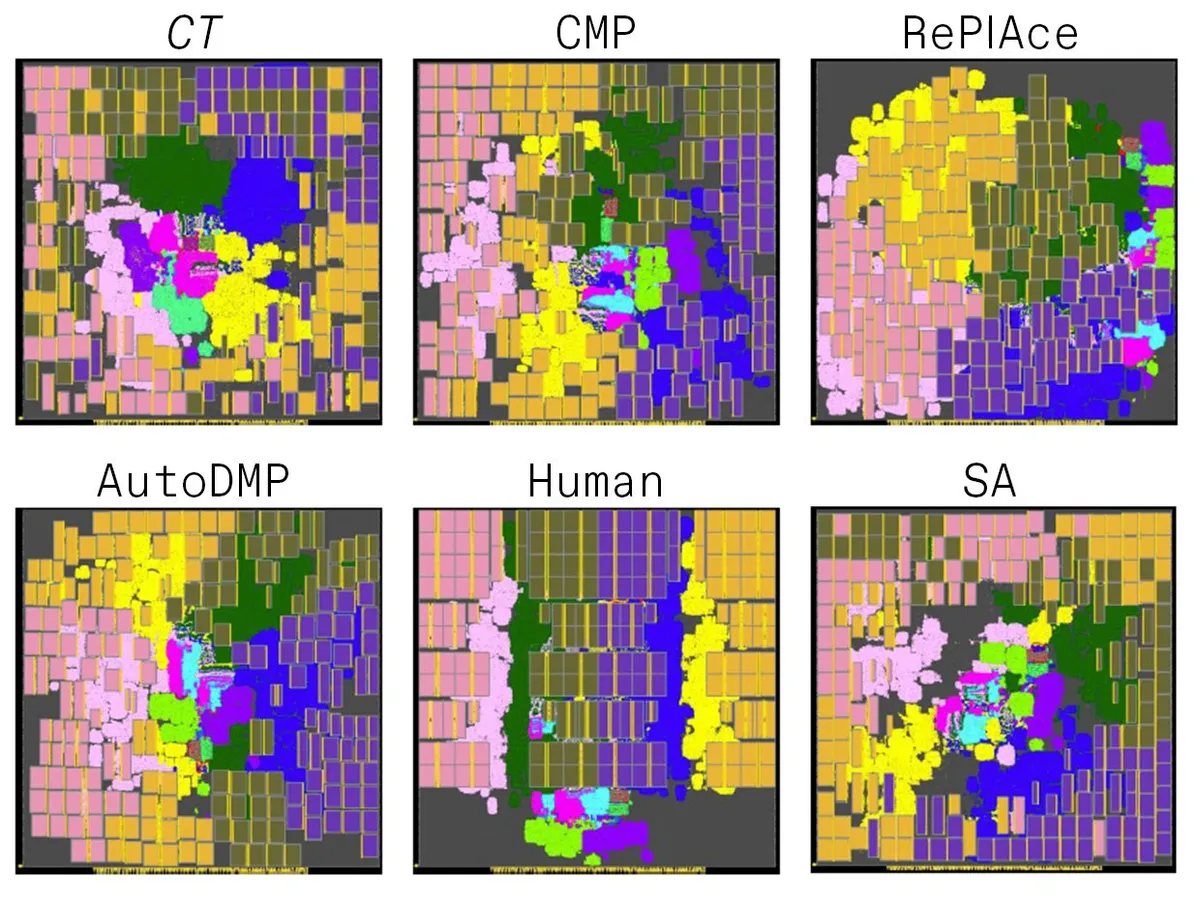
Same chip, six different placement methods: Circuit Training, CMP, RePLAce, AutoDMP, Human Expert, and Simulated Annealing. Each produces a wildly different layout. Only one closes timing.
The Proxy Metric Trap
Most AI research in this space focuses on macro placement, optimizing a proxy metric like half-perimeter wirelength (HPWL). The assumption: shorter wires, better chip. It's reasonable, but wrong often enough to be dangerous.
Placements with beautiful HPWL scores fall apart when you route them and try to close timing. Optimizing for short connections packs macros tightly, creating routing congestion. Wires compete for the same metal tracks. The clock tree bloats. Timing degrades. Power explodes.
The proxy metric said "great." The silicon said "no."
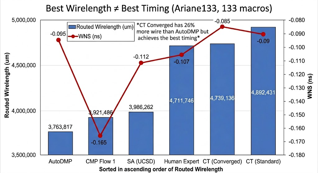
Ariane133 benchmark (133 macros). Sorted by wirelength, the "best" placement has the worst actual timing. The best timing comes from a placement with 26% more wire. Proxy optimization alone is insufficient.
Placement as a standalone optimization problem has a fundamental limitation. Even the best RL agent for placing macros won't tell you whether the chip actually works. That answer comes from the full backend flow, and that's the part that hasn't been automated.
What a Senior PD Engineer Actually Does
Most placement research stops at placement. But what happens after is where designs succeed or fail.
A senior PD engineer places macros, then runs CTS. Reads the clock skew report. Checks if buffers are creating congestion in layer M4. Looks at the IR drop heatmap. Notices two SRAMs near the clock root causing hold violations on 200 paths. Moves one SRAM 50 microns east, widens the power strap, re-runs.
This is reasoning, not optimization. Diagnosis, memory, judgment, informed by years of experience with how physical effects cascade through a design. No proxy metric encodes "the power grid can't handle two SRAMs drawing peak current in the same quadrant." These are emergent effects that only reveal themselves deep in the backend flow.
Placement is only 20% of the problem. The other 80%, clock tree synthesis, routing, timing repair, power integrity, is where chips actually ship or don't.
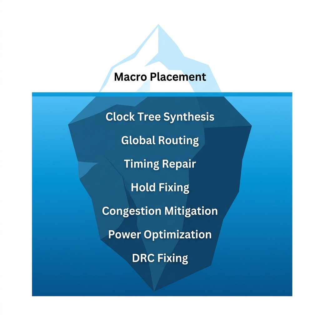
What AI placement research focuses on, and everything below the surface that actually ships a chip.
The Reasoning Layer of Chip Design
The EDA industry has evolved in phases. First, mathematical convergence: unified data models for timing agreement. Then, optimization convergence: RL and ML squeezing better PPA from individual steps.
What's missing is the reasoning layer. A system that understands the cascading physics of a real backend flow. That knows a wirelength improvement means nothing if it causes congestion three steps downstream. That remembers a strategy failed on a similar design last week and adjusts before wasting four hours of compute.
Our models don't predict what a good placement looks like. They understand why a placement fails, and what to do about it, across the full stack from floorplan to signoff. This requires training on real backend outcomes, real timing cascades, real power integrity failures. That data doesn't exist in any public dataset. We generated it ourselves: thousands of full-flow runs across dozens of real designs, each producing the ground-truth signal that proxy metrics miss.
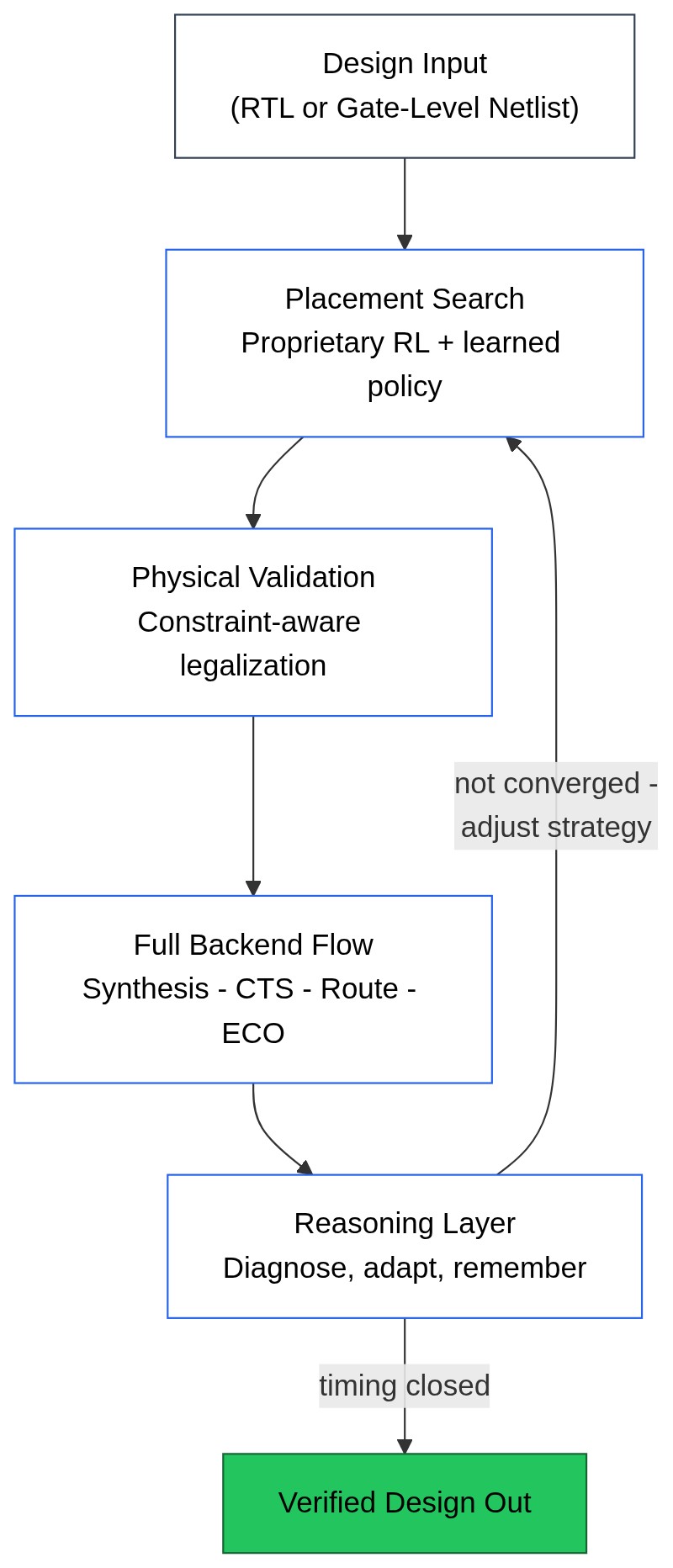
Proprietary RL explores the design space. The backend provides ground truth. The reasoning layer diagnoses, adapts, and remembers. No human in the loop.
What We're Building at ArchGen
AI should own the full physical design loop, not just one step.
Our system drives a design through the entire backend flow autonomously. It places, runs the real backend, reads the real reports, reasons about what went wrong, and iterates with memory of every previous attempt. The closed-loop intelligence of a senior PD engineer, running continuously and exploring the design space far more aggressively than any human can.
We've closed timing on real-world processor cores with over 100 macros. Real SoC subsystems with real PDK constraints and real timing signoff.
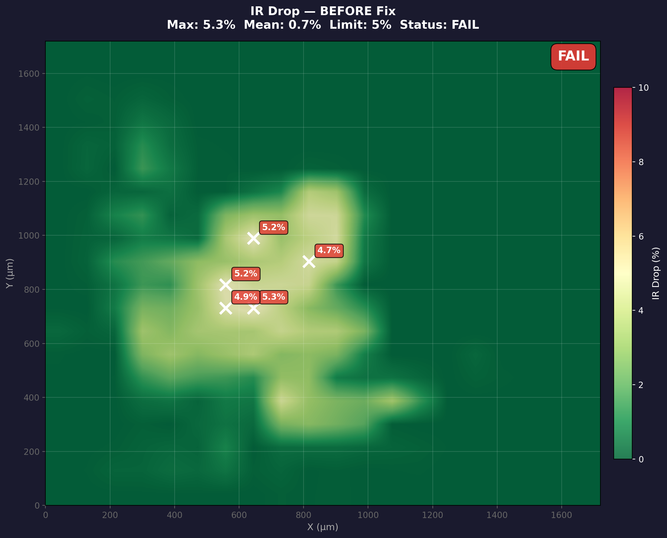
Before: IR Drop FAIL (5.3%, over limit)
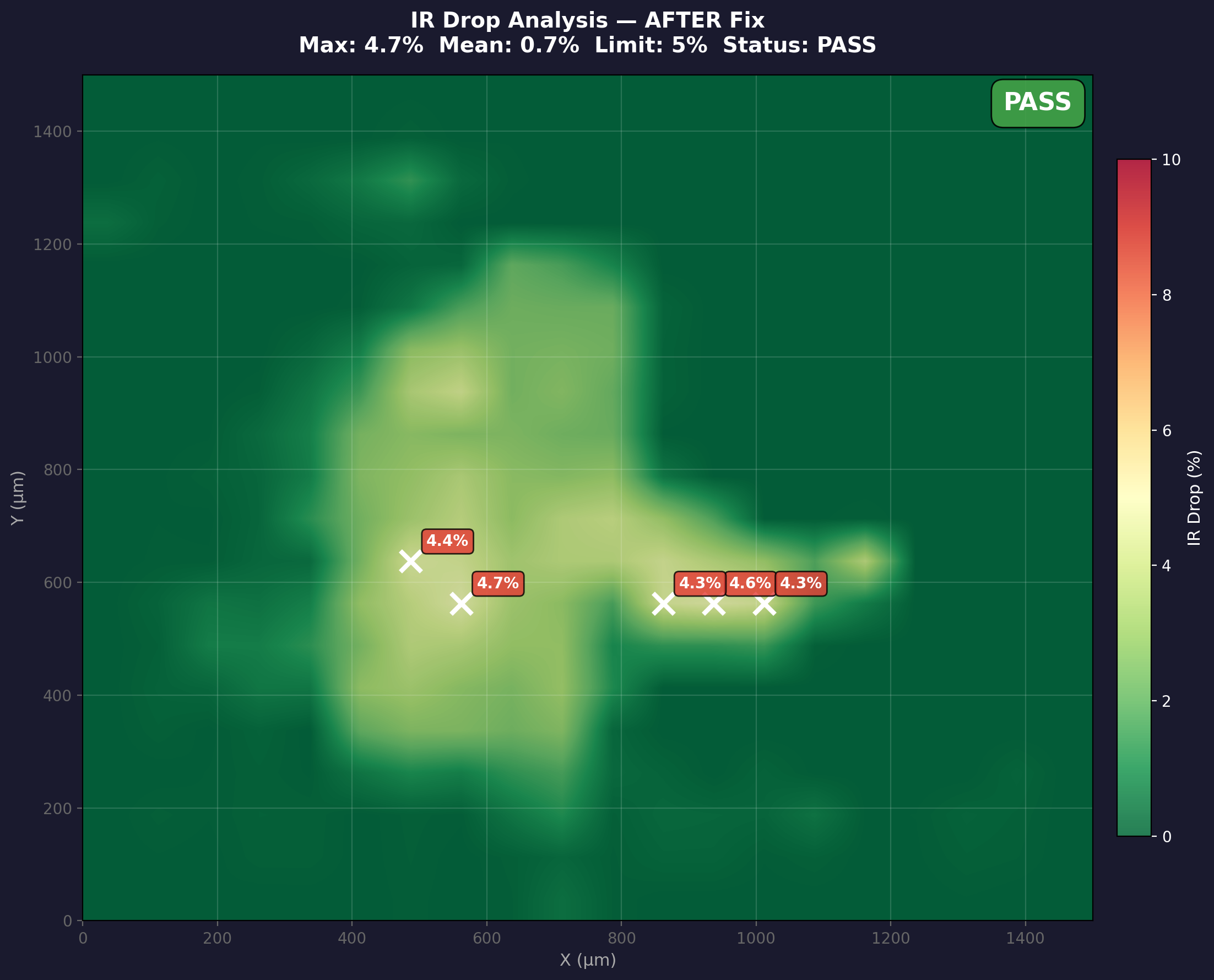
After: IR Drop PASS (4.7%, under limit)
Real power analysis heatmaps from our pipeline. Left: initial placement causes IR drop hotspots exceeding the 5% limit. Right: AI-optimized placement brings all hotspots under threshold.
The Road Ahead
The semiconductor industry is facing a capacity crisis. More chips need to be designed for AI accelerators, automotive, IoT, edge computing. There aren't enough physical design engineers. TSMC's revenue is growing 30% year-over-year. The EDA workforce isn't.
The answer isn't replacing engineers. It's amplifying them. A single PD engineer with the right AI should do what a team of five does today. Close timing faster. Ship designs in weeks instead of months.
The frontend got Cursor and Copilot. Physical design deserves the same leap. That's what we're building.
If you're working in chip design and want early access, visit archgen.tech.